Voltage margin
Review the maximum drain-source voltage, including switching overshoot and input transients, against the VDS rating.
DC POWER CONVERSION
Review switching devices, rectification and optional linear post-regulation against the input range, load and thermal requirements of a DC power design.
Explore component selectionFUNCTIONAL OVERVIEW
DC input
Operating range & transients
Switching stage
MOSFET, gate drive & topology
Regulated output
Load range & thermal evaluation
Functional overview of a converter. Inductors, capacitors, control and protection circuits are omitted.
APPLICATION OVERVIEW
DC/DC conversion adapts one DC voltage to another. The topology, input range, load current and control scheme determine how the switching devices are used.
A part number's voltage and current ratings are only the start. Gate drive, on-resistance conditions, switching characteristics and board-level thermal behavior all belong in the selection brief.
DESIGN CONSIDERATIONS
Review the maximum drain-source voltage, including switching overshoot and input transients, against the VDS rating.
Use RDS(on) values measured at a gate voltage relevant to the design. Gate threshold voltage describes the onset of conduction, not the fully enhanced on-state.
Consider conduction losses alongside gate charge and switching behavior. Compare values only with their measurement conditions in view.
Review pinout, footprint, mounting conditions and the available heat path. Datasheet current ratings do not automatically describe the current a finished PCB can sustain.
COMPONENT SELECTION
Compare low- and medium-voltage MOSFETs against the actual switch voltage and gate drive. Schottky rectifiers may be relevant to an asynchronous stage; an LDO may be evaluated separately for a lower-noise auxiliary or post-regulated rail. These are different circuit functions, and the linked devices are starting points for datasheet review.
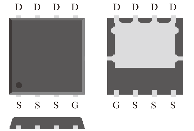
PDFN5*6
NTS036N03P530 V N-channel enhancement-mode trench MOSFET in a PDFN5*6 package, with a 112 A drain-current rating under the datasheet conditions. On-resistance values below retain their gate-drive and test-current conditions.
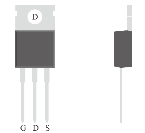
TO-220C
NTH084N06C60 V N-channel enhancement-mode trench MOSFET in a TO-220C package, with a 73 A drain-current rating under the datasheet conditions. On-resistance values below retain their gate-drive and test-current conditions.

TO-263
NTS096N08D80 V N-channel enhancement-mode trench MOSFET in a TO-263 package, with a 96 A drain-current rating under the datasheet conditions. On-resistance values below retain their gate-drive and test-current conditions.
CONTINUE EXPLORING
FUNCTIONAL OVERVIEW
AC input
Input bridge
Converter & output
POWER CONVERSION
Start at the input bridge, then examine the rectification and switching requirements of the converter and its output stage.
Explore applicationFUNCTIONAL OVERVIEW
AC input
Bridge rectifier
Driver & LED load
DRIVER & POWER SUPPLY DESIGN
Explore input rectification and component requirements for LED driver power supplies, with attention to package size and operating temperature.
Explore applicationLET'S DISCUSS YOUR APPLICATION
Explore the catalog or share your component requirements.