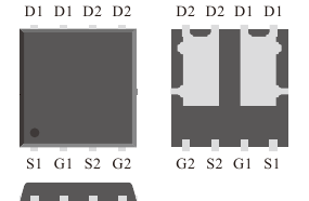
PDFN5*6D · Datasheet illustration
Dual N-channel MOSFETs
NSS230M10P5D
100 V dual N-channel MOSFET. The datasheet specifies 35 A for the channel under its stated thermal conditions and 29.3 mΩ maximum on-resistance at 10 V gate drive.
MOSFET configuration
Two N-channel MOSFETs
Conditions
Two independently gated N-channel devices shown in the connection diagram.
VDS, N-channel
100 V
Rating
Conditions
N-channel drain-source absolute maximum rating; TA = 25 °C.
ID, N-channel
35 A
Rating
Conditions
N-channel continuous drain current at TA = 25 °C as printed. Pulse width is limited by junction temperature; consult thermal curves. This is not a combined package current.
Product status: MP
PRODUCT OVERVIEW
A closer look at NSS230M10P5D.
100 V dual N-channel MOSFET. The datasheet specifies 35 A for the channel under its stated thermal conditions and 29.3 mΩ maximum on-resistance at 10 V gate drive.
- Two N-channel devices
- Separate gate and source terminals
Technical specifications
- MOSFET configuration
Two N-channel MOSFETs
Two independently gated N-channel devices shown in the connection diagram.
Datasheet p. 1- VDS, N-channel
100 VRating
N-channel drain-source absolute maximum rating; TA = 25 °C.
Datasheet p. 1- ID, N-channel
35 ARating
N-channel continuous drain current at TA = 25 °C as printed. Pulse width is limited by junction temperature; consult thermal curves. This is not a combined package current.
Datasheet p. 1- RDS(on), N-channel at 10 V, max
29.3 mΩMaximum
VGS = 10 V; ID = 17.5 A; TA = 25 °C.
Datasheet p. 2- Gate-source voltage rating (VGS)
-20 to 20 VRange
Gate-source absolute maximum rating.
Datasheet p. 1- Junction temperature range
-55 to 150 °CRange
Junction temperature range.
Datasheet p. 1
Values apply under their stated conditions. The datasheet includes the complete ratings, curves and package information.
Documents & downloads
NSS230M10P5D datasheet
PDF · English · A/1 · 2014-10-20