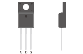
TO-220FP · Datasheet illustration
SiC MOSFETs
NCH75R130F
750 V N-channel silicon carbide MOSFET. Maximum on-resistance is 160 mΩ at VGS = 18 V and ID = 11.3 A. Refer to the datasheet for gate-drive, thermal and switching limits.
Drain-source voltage (VDS)
750 V
Maximum
Conditions
Drain-source absolute maximum rating.
Continuous drain current (ID)
19.5 A
Rating
Conditions
Continuous drain current at TA = 25 °C as printed. Pulse width is limited by junction temperature; consult thermal and safe operating limits.
RDS(on) at 18 V, max
160 mΩ
Maximum
Conditions
VGS = 18 V; ID = 11.3 A; TJ = 25 °C. Test condition, not a recommended gate-drive setting.
Product status: MP
PRODUCT OVERVIEW
A closer look at NCH75R130F.
750 V N-channel silicon carbide MOSFET. Maximum on-resistance is 160 mΩ at VGS = 18 V and ID = 11.3 A. Refer to the datasheet for gate-drive, thermal and switching limits.
- Silicon carbide N-channel MOSFET
Technical specifications
- Drain-source voltage (VDS)
750 VMaximum
Drain-source absolute maximum rating.
Datasheet p. 1- Continuous drain current (ID)
19.5 ARating
Continuous drain current at TA = 25 °C as printed. Pulse width is limited by junction temperature; consult thermal and safe operating limits.
Datasheet p. 1- RDS(on) at 18 V, max
160 mΩMaximum
VGS = 18 V; ID = 11.3 A; TJ = 25 °C. Test condition, not a recommended gate-drive setting.
Datasheet p. 2- Gate-source voltage rating (VGS)
-10 to 22 VRange
Gate-source absolute maximum rating. This differs from the operating gate-drive range.
Datasheet p. 1- Power dissipation (PD)
82 WMaximum
Maximum power dissipation; TA = 25 °C as printed; consult thermal derating.
Datasheet p. 1- Junction temperature range
-55 to 175 °CRange
Operating junction temperature range.
Datasheet p. 1
Values apply under their stated conditions. The datasheet includes the complete ratings, curves and package information.
Documents & downloads
NCH75R130F datasheet
PDF · English · A/1 · 2025-10-20